Institute for Compound Semiconductors supports business growth
11 April 2022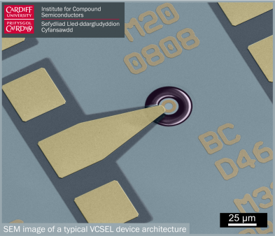
Cardiff University’s Institute for Compound Semiconductors (ICS) will move to a bespoke cleanroom this summer, working alongside business partners to help address a global shortage of semiconductor chips.
As a founder partner of CSconnected, the world’s first Compound Semiconductor cluster, the ERDF-funded ICS will collaborate with companies to develop, characterise and test new CS devices.
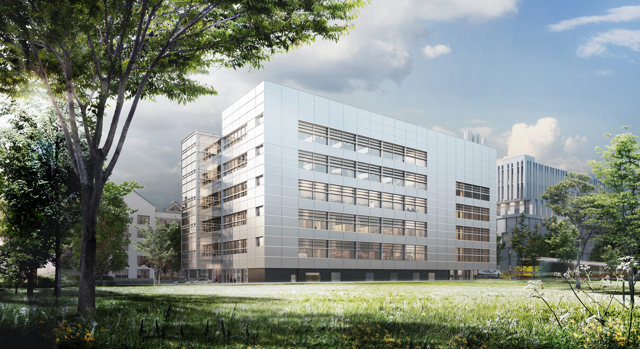 The purpose–built 1500m2 cleanroom, next door to the Translational Research Hub on the University’s Innovation Campus, will allow the ICS to provide a small to medium scale fabrication capacity to complement activity at other CSconnected partners , with the expertise and capability to translate academic excellence through to practical, manufacturable devices with the aim of generating economic impact through commercial and academic exploitation of CS technologies
Compound Semiconductors are critical components across a wide range of new technologies. The Cluster aims to develop a competitive advantage in key enabling technologies which will allow the UK to increase trade globally in critical sectors such as optical communications, 5G, autonomous and electric vehicles, aerospace, robotics and medical devices.
When ICS moves to the TRH and Clean Room in June, with an expanded workforce and new equipment, researchers will be able to process CS wafers up to 8” in diameter.
The spread of 5G technologies, the rise in working from home and a growth in products using fingerprint identification and image sensing means global demand for 8” wafer production continues to grow.
ICS is keen to work with businesses of all sizes, from major corporates to SMEs. With all processes under one roof, the ICS is an ideal development partner for start-ups working on new projects.
The Institute has established a range of robust VCSEL processes on wafer platforms up to 150 mm. Tiny chips that are used for high-speed communications in mobile phones and cars, VCSELs are Compound Semiconductor-based laser diodes that emit light vertically from their top surface, and can be produced in batches of thousands in a single wafer. Recently, using an in-house 6” process flow, five wafers were patterned to produce 20 tiles with 9 arrays of 100 devices on each, giving a total of 18,000 VCSEL devices. The five wafers were processed over 15 days and completed on time for our customer.
The ICS also provides the opportunity to collaborate with customers in the development and realisation of more bespoke VCSEL architectures, based upon our established in-house VCSEL process lines on GaAs and Ge substrates up to 150 mm diameter, with 200 mm currently in development.
A year of expansion lies ahead. With new equipment and freshly-recruited process engineers, ICS will relocate a cleanroom five times larger than its current home. In turn this enables scale-up of our process lines to accommodate 200mm wafer platforms.
Whatever size your business, if you’re interested in working with ICS, then please get in touch. Come and join us.
For more details, visit: www.cardiff.ac.uk/institute-compound-semiconductors or email ICS@cardiff.ac.uk, follow us on twitter @ICSCU
