Developing Net Zero Solutions
2 October 2023
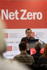
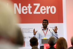
The Institute for Compound Semiconductors at Cardiff University’s Translational Research Hub (TRH) works with industry to develop Net Zero solutions. At the Hub’s recent launch event, two researchers – Dr Bo Hou and Dr Naresh Gunasekar, both from the Condensed Matter and Photonics Group in the School of Physics and Astronomy – explained their work on energy-efficient Compound Semiconductor devices.
Dr Bo Hou
“I want to talk to you about two very important technologies: energy efficient lighting and solar cells. Every month, when we get our electricity bills, we always complain of price increases. If we can switch to energy efficient lighting technologies, we can massively reduce our costs.
Compared to traditional lighting, LED technology can reduce energy consumption by 80 per cent. Solar cells can generate power for free. Both LED and solar are underpinned by semiconductor technologies, and future energy-efficient technologies will need compound semiconductors.

In my own research group, we are particularly interested in making very special compound semiconductors through a process called nanofaceting – the formation of small, flat surfaces on nanoparticles to manipulate quantum dots into a variety of shapes called nanocrystals.
These nanocrystals have unique optical and electronic properties, which can be used in different types of technology and have the potential to revolutionise a number of industries because of the theoretically limitless efficiencies they offer.
Our study is a significant step forward in the adoption of quantum dots technology across a wide range of energy and lighting industry applications.
We imagine the truncated octahedra we manufactured might in future be used for energy harvesting in solar cells, improving efficiencies beyond the capabilities of current technologies which sit at around 33%.
Likewise, our nanocrystals might be used for biomedical imaging, where inefficiencies and instabilities are currently limiting their use in diagnoses and drug delivery.”
Dr Naresh Gunasekar
“I work on wide band gap materials for compound semiconductors. Of all our energy use, 40 per cent goes on electricity, and 20 per cent goes on lighting, so if you can make energy efficient material and use it for devices then we can save a lot of energy.
My research looks at wide band gap materials – how can we make much more compact devices, which are really useful for energy efficiency?

You’ll have heard the phrase ‘the blink of an eye.’ The real blink of an eye takes roughly one-tenth of a second, but wide band gap materials are 10 billion times quicker.
To give you an example, my work focuses on manufacturing these devices, and understanding processes: how to make them more efficient and more cost-effective as well.
For this, you need to test the devices and understand how to make them more efficient and cost-effective.
So, within our research group we have techniques which can help us understand quicker processes in semiconductor materials. Thanks to research infrastructure funds, we have now established systems in our TRH building, working with the CCI (Cardiff Catalysis Institute) and using the Cleanroom facility where we can make these devices, understand their properties and test them. I’m very excited by the prospects of the TRH and look forward to working with the Institute within the Hub.
Thank you.”

For more information about the Institute for Compound Semiconductors, visit our website, or watch our film, below, about the newly launched ICS Cleanroom 👇👇👇.
If you are interested in learning more about the work of the Net Zero Innovation Institute, our strategic areas and vision, as well as how you can contribute to Net Zero research at Cardiff University, visit our website at https://www.cardiff.ac.uk/net-zero-innovation-institute and follow us on Twitter – @CUNetZero.