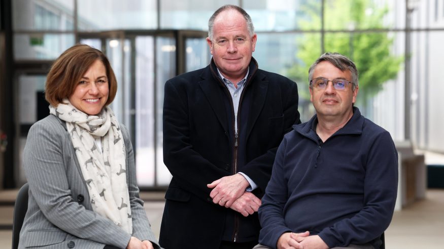
Kubos Semiconductors: lighting the way with microLED innovation
24 October 2024
From smartphones and tablets to satellite communications and GPS, compound semiconductors drive the devices and technologies we use today. Kubos Semiconductors are pioneering new research breakthroughs and developments in this vital area.
Compound semiconductors play a crucial role in modern technology, as they emit and receive light, operate in high-power applications, and are integral to quantum technologies, which will become increasingly important in future applications like AI, machine learning, and robotics.
Kubos Semiconductors is a leader in semiconductor innovation, focusing on advanced LED technology. They specialise in cubic Gallium Nitride (GaN) materials, which boost the efficiency and performance of LEDs, especially red microLEDs. This technology solves major issues like the low efficiency of red microLEDs, important for augmented reality (AR) and virtual reality (VR) devices as they’re essential for creating vivid and immersive displays.
Kubos Semiconductors joined the Cardiff Innovations community at sbarc|spark earlier this year. Here, we speak to CEO Caroline O’Brien, a semiconductor industry specialist, about the work Kubos Semiconductors is doing, and what this location in the heart of the Cardiff University campus means for them.
What we do
“Kubos Semiconductors is developing Cubic GaN, a novel compound semiconductor material. This patent protected material has unique physical properties which offer significant cost and performance advantages over the established technology for green and red microLEDs.
Initially aimed at visible light LED applications and displays, as a panacea for more efficient red microLED in AR/VR applications and displays, it could also be used in communications, power electronics and radio frequency in the future. The material is epitaxially grown using standard industry equipment and processed on 150mm wafer diameter silicon substrates, but scalable to 200mm and beyond.”
Our new home
“Bringing Kubos Semiconductors closer to our partners and becoming part of the South Wales Compound Semiconductor Cluster is an important next step on our journey, particularly as we are a fabless semiconductor company.
This office location in sbarc|spark means we are very near to where we grow our epitaxial material and process our LEDs at the Institute of Compound Semiconductors, based at the Translational Research Hub. It affords us access to a wealth of academic expertise and advanced research facilities, which will undoubtedly lead to more groundbreaking innovations in GaN technologies, pushing the boundaries of what is possible in semiconductor performance and efficiency.
It also offers the potential for us to integrate with other state-of the art companies leading innovation in the UK and will no doubt help accelerate our development plans.”
What’s next
“Kubos is focussing on preparing the world’s first red microLED demonstrator using cubic GaN for launch at Display Week 2025. In addition, we will provide updates on collaborations with industry partners and commercial engagements throughout 2025, as we improve the material efficiency and further our product roadmaps.”
Find out more
Learn more about the work Kubos Semiconductors is undertaking by visiting their website, or following them on LinkedIn.
Discover the opportunities available in Cardiff Innovations labs, offices, and co working spaces.