New cleanroom for CS technologies
9 August 2021
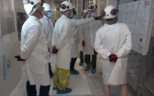
Scientists who will work in Cardiff University’s state-of-the-art Compound Semiconductor (CS) cleanroom have visited their future home.
 Researchers from the ERDF-funded Institute for Compound Semiconductors (ICS) were given a tour of the facility, which will offer an 8-inch wafer fabrication line to cope with growing demand for CS devices.
The Cleanroom is being delivered by Ardmac – the leading provider of high-tech cleanrooms – and forms a key part of Cardiff University’s new Innovation Campus, which combines cutting-edge research, technology transfer, business development and student enterprise.
The Institute has received substantial funding for its new building and equipment including over £30 million of external investment. In addition to the 1,500 square metre cleanroom, a dedicated characterisation room and back-end processing areas will enable the ICS to process wafers up to 8-inches in diameter and expand its range of industry-standard services.
Reacting to the site tour, Chris Matthews, ICS Project Manager (WEFO), said: “I started working on the business plans in late 2015/ early 2016, so to go from seeing it on the drawing board to being in the physical building is just an amazing journey really. Compared to our current accommodation in Cardiff University’s Queens Building, we’ll have room to expand and do bigger and better things.”
 The ICS itself will be based in a bespoke Translational Research Hub next to the Cleanroom. The Hub offers new office accommodation, shared, interactive working zones, laboratories, and breakout spaces. The TRH is designed to bring researchers and industry professionals closer together, creating a working environment that attracts and retains talented researchers.
The ICS will share the Innovation Campus at Maindy Road with Cardiff Catalysis Institute, the Social Science Research Park (SPARK), and Cardiff innovations@sbarc, a creative base for start-ups and spinouts.
The Institute will have access to shared facilities with its neighbours, including a TEDx-style auditorium and fabrication lab to trial new manufacturing technologies.
Compound semiconductors are high-speed electronic chips. Composed of elements either side of those in group IV of the periodic table (eg groups III and V), they are 100 times faster than silicon, and have the ability to emit and sense light, all the way from the infrared, through the visible and into the ultra-violet part of the spectrum.
CS technologies have already complimented silicon in areas such as wireless communications, where chips made from material combinations such as gallium and arsenic (gallium arsenide, or GaAs) are found in virtually every smartphone, enabling high speed, high efficiency wireless communications in cellular and WiFi networks.