Illuminating breakthroughs
11 February 2021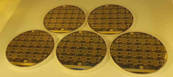
The trials of 2020 spurred scientists worldwide to overcome challenges. Despite restricted operating restrictions, experts at Cardiff University’s Institute for Compound Semiconductors (ICS) ended the year by successfully demonstrating their ability to process multiple 6” compound semiconductor wafers on specification, and on time, to a customer. Here, ICS Director, Professor Peter Smowton, outlines the achievement.
 “It’s a year that will live long in the memory. Bringing disruption and an adjustment to working patterns, the 2020 pandemic led to full closure of the ERDF-funded ICS from the end of March until July.
We gradually re-opened the facility but with reduced working hours and occupancy of its cleanroom, maintaining social distancing throughout. Despite this, our ambition to scale up wafer production drove our small clean room team onwards as the ICS maintained its professional support and expertise to users in the University, the CSConnected cluster, and beyond.
The team worked tirelessly. Their continued dedication was demonstrated just prior to the Christmas break when the cleanroom team successfully completed their first multi-wafer fabrication run of 6” wafers within its 225m2 Queen’s Buildings cleanroom.
The batch consisted of one demonstration wafer immediately followed by five top-side emitting VCSEL (Vertical Cavity Surface Emitting Laser) wafers, all designed to emit at 940nm.
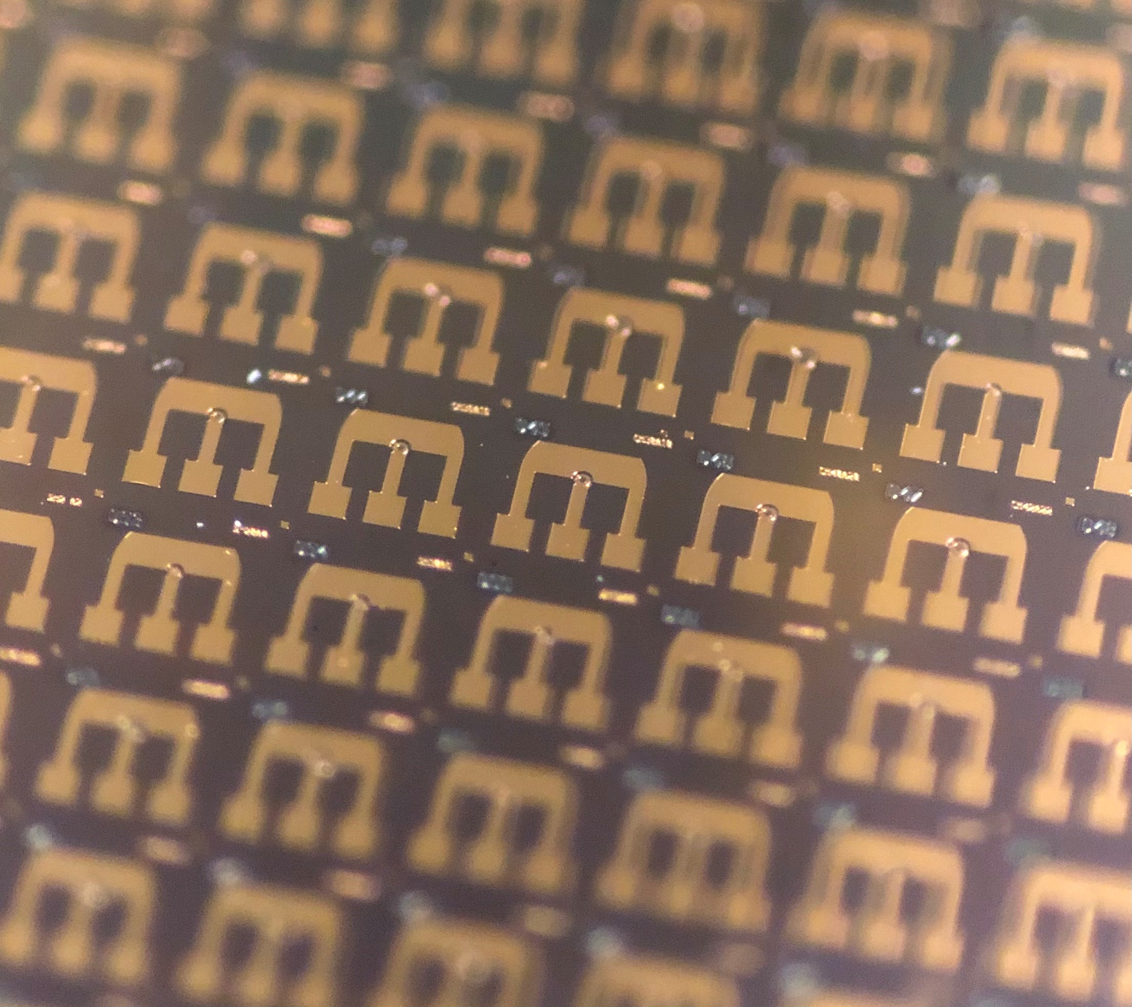
VCSELs are tiny chips used in high-speed communications like mobile phones and cars. As semiconductor-based laser diodes that emit light vertically from their top surface, they can be produced in batches of thousands in a single wafer.
Using our in-house 6” process flow, each wafer was patterned to produce 20 tiles with 9 arrays of 100 devices on each, giving a total of 18,000 VCSEL devices and additional test structures. We produced five wafers, processed over 15 days, and all completed on time.
The wafers were then passed to our colleagues working on the KAIROS project and on the Cardiff-based EPSRC-funded CS Hub for characterisation, where results have shown successful device operation across all the wafers.
Proving our 6” wafer production process is an excellent achievement for the ICS team working within its existing Queen’s facility, especially given current limitations.
Above all, it augurs well for the future when, in mid-2022, we will relocate to a new purpose–built 1500m2 cleanroom on the University’s Innovation Campus. There the ICS staff will be located alongside the clean room in the Translational Research Hub, complete with bespoke laboratories and offices.
Once there, with an expanded workforce and new equipment, the ICS will be able to process CS wafers up to 8” in diameter for which there is an increasing demand. The spread of 5G technologies, the rise in working from home and a growth in products using fingerprint identification and image sensing means the demand for 8” wafer production continues to illuminate the Compound Semiconductor industry in 2021.”
Professor Peter Smowton, Director, Institute for Compound Semiconductors
Comments
1 comment
Comments are closed.
Well done to ICS team! A step closer to 8″ wafers.